 Business License

How Zirconia Sputtering Targets Unlock Extra Profits for Production Lines
On photovoltaic, battery and semiconductor production lines, sputtering target failures can turn into a major cost‑consuming pitfall:
‑ Will uniformity fluctuations result in batch‑level scrap?
‑ Will shortened service life cause frequent production shutdowns?
‑ Will long import lead‑times hold back production scheduling?
Is there a sputtering target that can maintain baseline performance and bring extra profits for production lines?
The answer lies in the solution offered by UV Tech Material LTD. (UVTM) — high‑purity zirconia sputtering target.
💡 Why zirconia among all sputtering targets?
▶️ High‑k dielectric constant to ease bottlenecks for advanced processesZirconia has a dielectric constant roughly six times that of silicon dioxide. In scenarios such as capacitor dielectrics for semiconductor memory devices and insulating layers for advanced packaging, it can effectively lower leakage current and boost device performance. It delivers a wider window for thin‑film design and larger process tolerance, which naturally stabilizes production yield.
▶️ Transformation‑toughening plus anti‑arcing, dual safeguards for production‑line stabilitySubjected to stress, zirconia triggers spontaneous crystal‑phase transformation to restrain crack expansion, granting it prominent crack‑resistant capability. Meanwhile, fine resistivity adjustment restrains charge accumulation under high‑power sputtering, greatly cutting the occurrence of micro‑arcing and nodule formation and reducing particle‑related defects from the source.
▶️ Thermal stability and chemical inertness for demanding process environmentsFor solid‑state batteries, zirconia thin‑films work as electrode modification layers and electrolyte barrier layers to lift cycle life and thermal safety. For photovoltaic modules, deposited anti‑reflection and passivation protective films reduce light reflection loss and enhance weather resistance.
💡 Two technical routes to satisfy full‑scenario demands
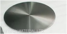
▶️ Planar Target: Adopting cold isostatic pressing and high‑temperature sintering, the process achieves high density and fine‑grain microstructure of targets. It substantially cuts particle generation and abnormal discharge during sputtering and brings immediate improvement in finished‑product rate. It fits rigorous fields including semiconductor high‑k dielectrics and high‑precision optical coating.
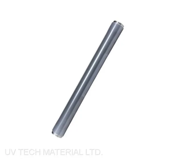
▶️ Rotary Target: One‑step forming via plasma spraying. It balances dimensional flexibility and coating density and enables the manufacture of large‑size rotary targets, perfectly matching continuous‑production requirements of large‑area coating lines for photovoltaic glass and Low‑E glass.
With both technical routes in place, UV Tech Material LTD. (UVTM) can work out custom‑tailored optimal solutions for each customer.
💰 Where do profits get saved?
✅ Saved on yield: Whether using sintering or spraying processes, UVTM implements strict quality control, greatly lowering batch scrap rate.
✅ Saved on downtime: Uniform and stable target structure notably extends service life, reduces target‑replacement frequency and grants more sufficient production time.
✅ Saved on lead‑time: Supported by in‑house production bases and mature dual‑process production lines for spraying and sintering, it realizes fast local delivery of zirconia planar and rotary targets. Customers achieve higher flexibility for production scheduling and better capital turnover efficiency simultaneously.
🏭 UV Tech Material LTD. (UVTM)’s sputtering target family covers more than zirconia:
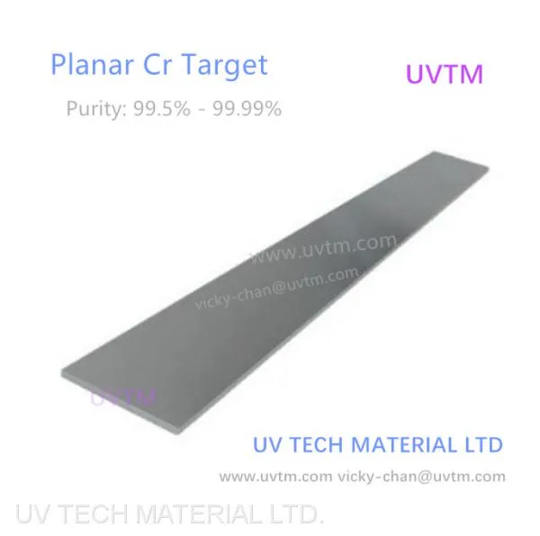
✅ Metallic Targets: e.g. silver, copper, aluminum and nickel targets. They serve as core conductive or reflective materials for semiconductor interconnection, photovoltaic thin‑films and large‑size Low‑E glass, featuring high purity, high density and fast film‑forming rate.
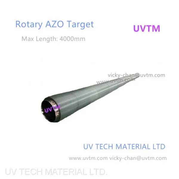
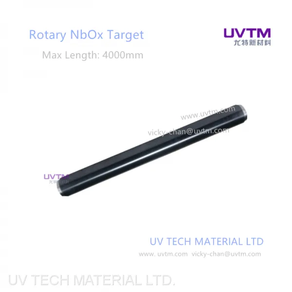
✅ Oxide Targets: e.g. zirconia, ITO, IGZO, AZO. They cover cutting‑edge sectors including semiconductors, solid‑state battery barrier layers, high‑resolution display panels and transparent conductive films, with extremely high technical barriers.
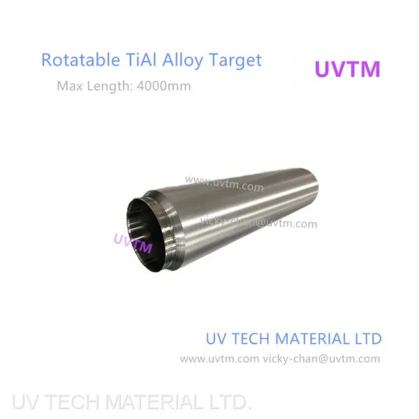
✅ Alloy Targets: e.g. silicon‑aluminum, tungsten‑titanium, nickel‑chromium, titanium‑aluminum targets. They are applied in advanced semiconductor packaging, energy‑saving glass and high‑end functional coatings, boasting precise composition and highly customizable performance.
✅ Ceramic Targets: e.g. alumina, silicon nitride targets and corresponding ceramic powders. They are used for semiconductor insulating dielectrics, cutting‑tool hard coatings and precision ceramic substrates, with high hardness and outstanding wear resistance.
👉 Why choose UV Tech Material LTD. (UVTM)?
✅ Years‑long R&D and manufacturing experience for sputtering targets, serving hundreds of enterprises
✅ Purity ≥99.7%, quality controlled from the source
✅ Mastery of two core processes: sintering and spraying; full coverage for planar and rotary targets
✅ Large‑scale standardized production bases with mature and stable supply chains
✅ On‑site technical support team available to assist with target mounting and process commissioning
Zirconia sputtering target acts as a high‑k barrier blocking electric leakage in semiconductor devices, a chemical shield fending off side reactions at solid‑state battery interfaces, and an optical anti‑reflection layer cutting reflection loss on the surface of photovoltaic modules. What UV Tech Material LTD. (UVTM) strives for is to convert material‑level irreplaceability into tangible profits shown on your production‑line bills.
📞 Feel free to leave a message or make an inquiry to obtain free technical consultation and sample trial services. UV Tech Material LTD. (UVTM), with precise craftsmanship, safeguards every one of your sputtering processes.
#ZirconiaSputteringTarget #SputteringTarget #SemiconductorMaterials #SolidStateBattery #PhotovoltaicCoating #HighkDielectric #PlanarTarget #RotaryTarget #DomesticSubstitution #UVTM
Recently Posted
-
High-Purity Silicon Aluminum Targets for Energy Storage and Smart Glass Manufacturing
August 28, 2026The stability of the global supply chain in vacuum deposition relies heavily on premium sputtering consumables. Accumulating over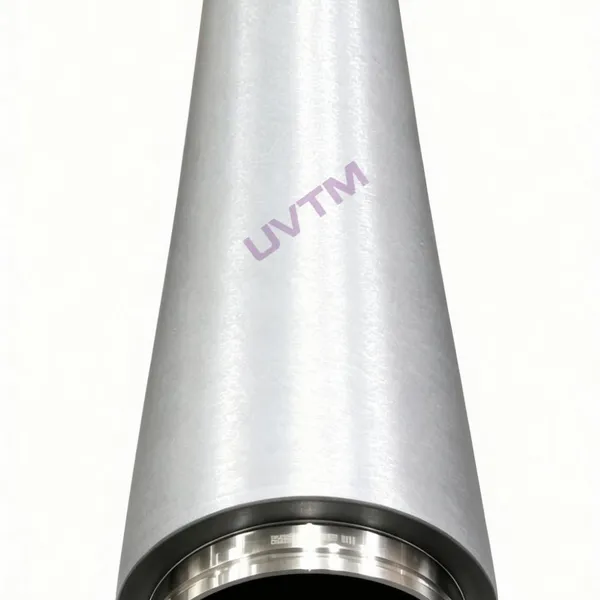 Read More
 -
Mass Production Ready: ≥99.9% Purity Ti-Si Rotary Targets for Semiconductor Deposition
August 27, 2026The stability of the global vacuum deposition supply chain relies heavily on premium sputtering consumables. The accumulation of o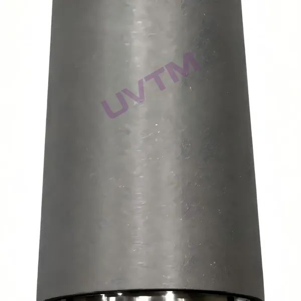 Read More
 -
Source Direct: High-Purity Ti-Al Targets for Advanced Vacuum Coating
August 26, 2026The stability of the global vacuum deposition supply chain relies heavily on premium sputtering consumables. Backed by over 100 pa Read More
 -
UV Tech Material LTD. High-Purity Indium Tin Target for Semiconductor & Display Deposition
August 25, 2026Guangzhou UV Tech Material LTD., as a dedicated manufacturer, provides advanced deposition solutions tailored for rigorous applica Read More

Contact Us
Recommended Products
-
 Rotatable NbOx Sputtering TargetUS$ 1000 - 20000MOQ: 2 Pieces
 -
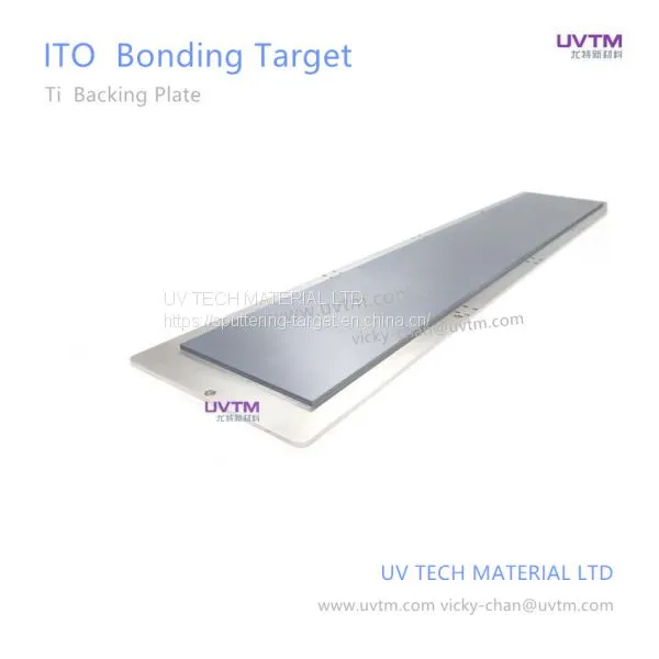
ITO Target 90:10 95:5 99.99 4N High Purity Planar Sputtering Target With Backing Plate Manufacturer Factory PriceNegotiableMOQ: 1 Set
-
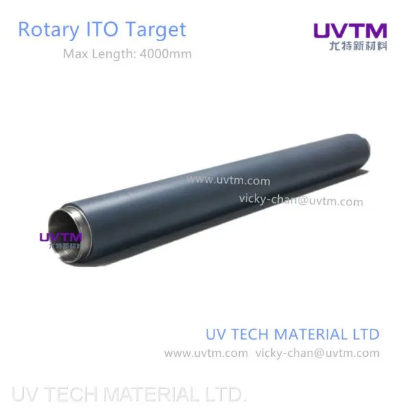
ITO Target 90:10 95:5 99.99 4N High Purity Rotary Bonding ITO Sputtering Target With Backing Tube Manufacturer Factory PriceNegotiableMOQ: 1 Piece
-
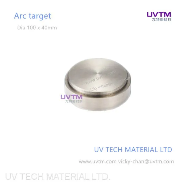
Arc Ti Target TiAl Cu Al Si Planar Sputtering Target for PVD Coating Thin FilmNegotiableMOQ: 10 Pieces
-
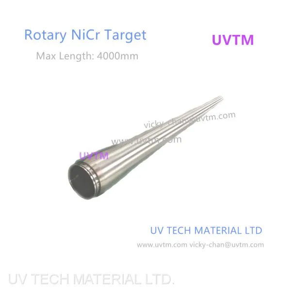
NiCr Target UVTM Alloy Target for Magnetron Sputter Coating Low e Glass Nano Thin FilmNegotiableMOQ: 2 Pieces
-
TiAl Target UVTM Alloy Target for Vacuum Sputter Coating TiAl Alloy Thin Film Made in ChinaNegotiableMOQ: 2 Pieces
-
Cr Target High Purity Planar Chromium UVTM Target Bonding Copper Backing Plate Factory PriceNegotiableMOQ: 2 Sets
-
AZO Target 98:2 99:1 4N High Purity Rotary Bonding AZO Sputtering Target With Backing Tube Manufacturer Factory PriceNegotiableMOQ: 1 Piece
-
NbOx Target Niobium Oxide Rotary Sputtering Target for Magnetron Sputter Low e Glass and Reflective Glass Coating Nano Thin FilmNegotiableMOQ: 2 Pieces
-
SiAl Target UVTM Alloy Target for Magnetron Sputter Coating SiO2 SiN4 Nano Thin FilmNegotiableMOQ: 2 Pieces